Hi @Daehan-Won
So, on the M0062 debug board, you do not need to connect an extra hub. You already have 3 USB ports...
Look at J10, J11, and J12..
https://docs.modalai.com/m0062-datasheet/#connector-callouts
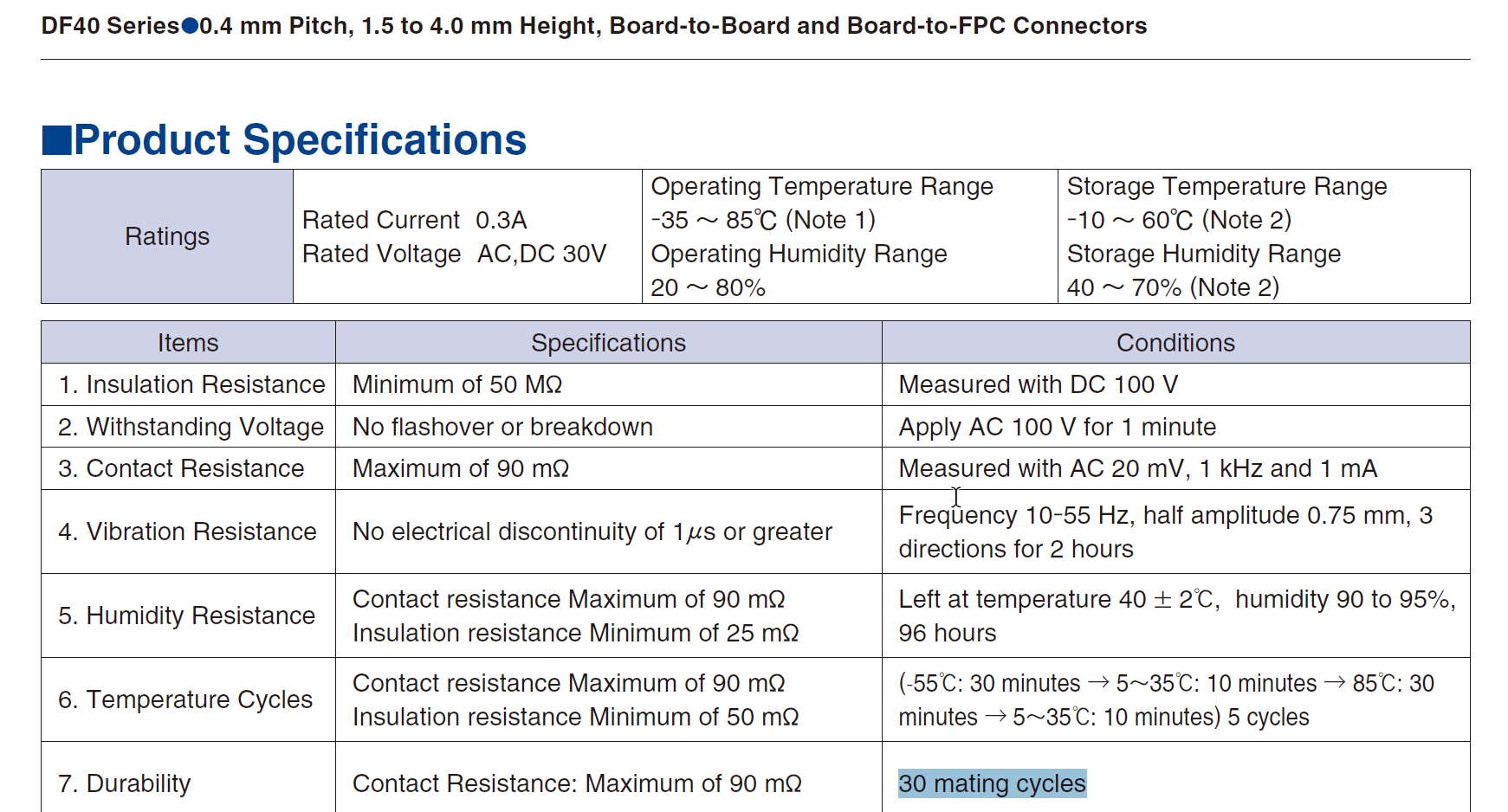
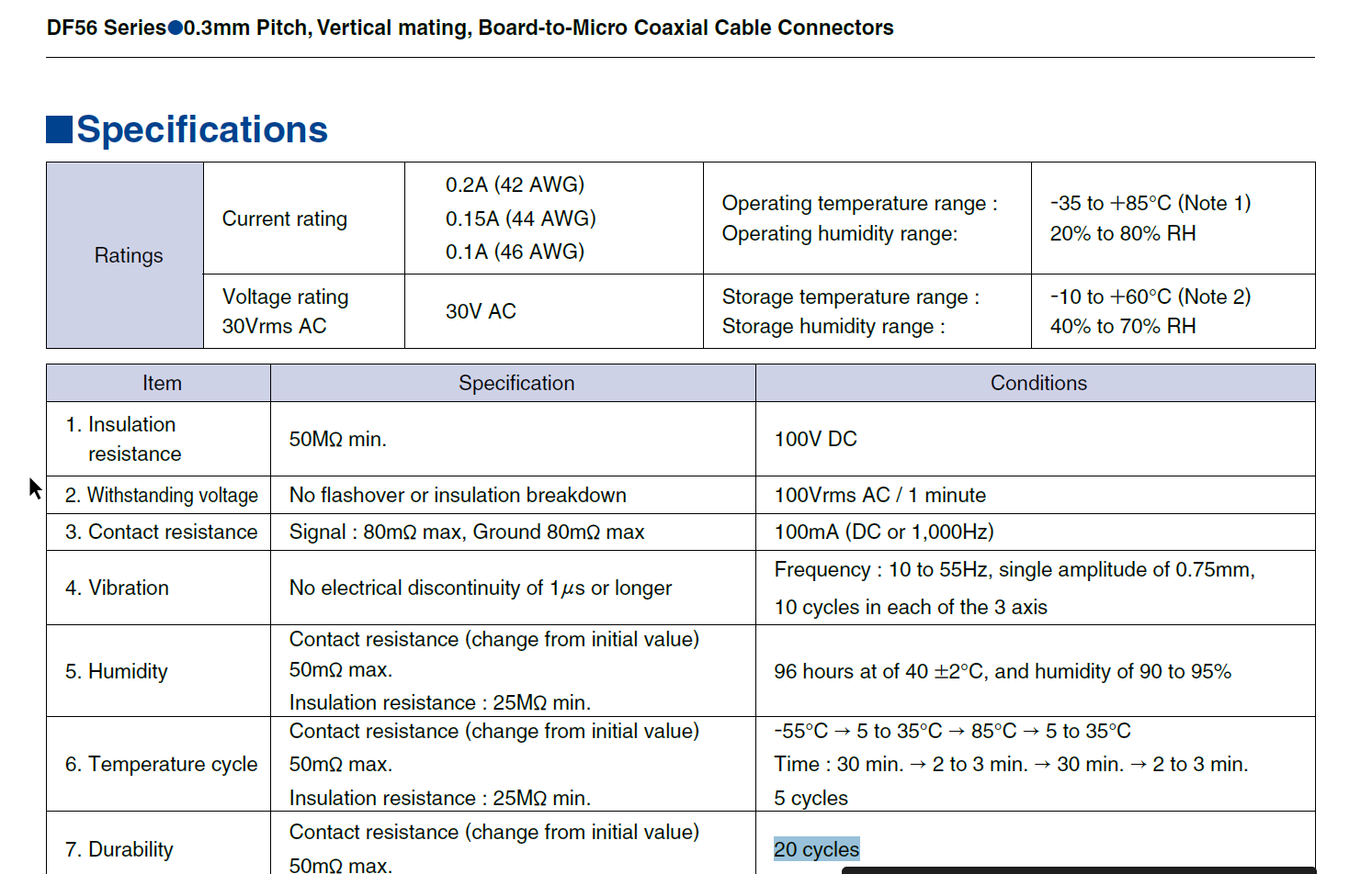
Yes they are different connectors, but is a much easier system for you. We sell both 4 and 10-pin USB cables, and you can easily get Type-A breakouts from Adafruit or Digikey.
Can you try to remove the extra hub and see if you can get your system to work that way?
We cannot validate or debug third party hardware/modules ... we would only be guessing and do not want to lead you down the wrong path. However, I suspect in this case, that Hub is indeed your issue. It is most likely only supporting 500mA modes, and if neither of those two devices are enumerating perfectly, it may only allow 100mA per port before tripping a reset. Depends on how it is configured and designed.
You can use USB TreeView to read all the descriptors of that hub board, and look for the self vs bus powered reporting, and the downstream current allocations. I suspect this is not set for your system.
If you use our connectors, despite in various formats, you should be much better off.
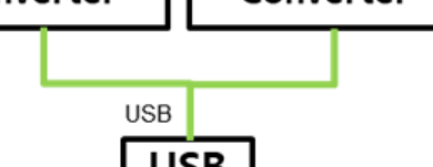
Lastly, just to clarify, are your USB connections unique? Your drawing looks like they are the same USBD+/D- wires connecting to one port of the Hub. 


