
FLIR LEPTON 3.5 Thermal camera with VOXL 2
-
@KLindgren thank you for reverting back. From which port are you taking the 3.3 V also how did you complete the circuit, the image you provide is confusing with respect to the connections, it would be great if you would provide further details.
@Jetson-Nano Our 2 Leptons are connected as described in this image - though we're using PureThermal boards instead of M0187s for the Leptons. The 3.3V VIN is provided from the VOXL's J19 port via this cable and a "Y" split jumper we've soldered together.
-
Hi @Jetson-Nano
Sch updates look correct. I'd still add a pull-up on the Lepton Reset to help control it during initial power-ON before the IO expander is configured.To help further debug your existing setup, I'd need more tangible info such as pictures with all your cables, etc. Do you have a DMM handy showing the voltages of 1.2V and 2.8V, and an O-scope for the 25MHz?
Can you also post a pic of your board without components installed (so I can review the layout as best as possible)?
It's hard to give much further guidance without actual hardware in my hands.
Thanks!Hi @Vinny, @Alex-Kushleyev,
Thank you once again for your valuable feedback on the schematics, and apologies for the delayed response.
I’ve now completed the PCB layout based on the updated schematics and newly selected components, as per your suggestions. I would greatly appreciate it if you could take a moment to review the layout and share your feedback—particularly on whether it meets the required configuration or if any modifications are recommended.
The following have been included in the shared Drive link:
Screenshots of all four layers
3D views of both the top and bottom sides of the board
 Drive link: https://drive.google.com/file/d/1czCx-N8ws3CelpKTV1VRBTzFZLcd-odx/view?usp=drive_link
Looking forward to your insights.
Thank you again for your continued support and guidance.
-
Hi @Vinny, @Alex-Kushleyev,
Thank you once again for your valuable feedback on the schematics, and apologies for the delayed response.
I’ve now completed the PCB layout based on the updated schematics and newly selected components, as per your suggestions. I would greatly appreciate it if you could take a moment to review the layout and share your feedback—particularly on whether it meets the required configuration or if any modifications are recommended.
The following have been included in the shared Drive link:
Screenshots of all four layers
3D views of both the top and bottom sides of the board
Drive link: https://drive.google.com/file/d/1czCx-N8ws3CelpKTV1VRBTzFZLcd-odx/view?usp=drive_linkLooking forward to your insights.
Thank you again for your continued support and guidance.
Hi @Jetson-Nano
I've been on vacation and just catching up. It will be a few days before I can get to this.
Thanks for your patience. -
Hi @Vinny, @Alex-Kushleyev,
Thank you once again for your valuable feedback on the schematics, and apologies for the delayed response.
I’ve now completed the PCB layout based on the updated schematics and newly selected components, as per your suggestions. I would greatly appreciate it if you could take a moment to review the layout and share your feedback—particularly on whether it meets the required configuration or if any modifications are recommended.
The following have been included in the shared Drive link:
Screenshots of all four layers
3D views of both the top and bottom sides of the board
Drive link: https://drive.google.com/file/d/1czCx-N8ws3CelpKTV1VRBTzFZLcd-odx/view?usp=drive_linkLooking forward to your insights.
Thank you again for your continued support and guidance.
Hi @Jetson-Nano
I do not have access to the link you have above.
Please reach out to us using the contact form https://www.modalai.com/pages/contact-us and we can get a more detailed review scheduled using your native cad tools which is more effective for us.Just mention in the form you wish to reach Vinny and then in the response from our team, you can reply with your data and they will forward it to me.
Thanks! -
Hi @Jetson-Nano
I do not have access to the link you have above.
Please reach out to us using the contact form https://www.modalai.com/pages/contact-us and we can get a more detailed review scheduled using your native cad tools which is more effective for us.Just mention in the form you wish to reach Vinny and then in the response from our team, you can reply with your data and they will forward it to me.
Thanks!Thank you for the update — I hope you had a great vacation!
As you mentioned, I’ve submitted an inquiry through your contact form. Once I receive a response from your team, I’ll follow up with the necessary details and additional data as needed.
Thank you for your continued support.
-
Thank you for the update — I hope you had a great vacation!
As you mentioned, I’ve submitted an inquiry through your contact form. Once I receive a response from your team, I’ll follow up with the necessary details and additional data as needed.
Thank you for your continued support.
Hi @Jetson-Nano
I received your data package and will review it this evening.
Thanks!
Vinny -
Hi @Jetson-Nano
I received your data package and will review it this evening.
Thanks!
VinnyHi @Jetson-Nano I have reviewed your schematic again and your layout files.
I cannot see any reason why your design will not work.
The only suggestion I have is to increase your capacitors here to 1uF:
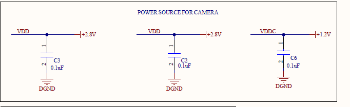
But, otherwise, your layout is OK (some improvements can be made, but nothing is detrimental):
- Pin 1 correct on connector, socket, LDO, other ICs
- Vias are picking up planes correctly
- Voids where expected
- Generous copper trace thickness
The one issue I think I might have found is your reference designators do not match the schematic between the layout. So, I'm wondering if you are installing parts from the BOM in incorrect locations...
For example, the cap on the output of the LDO is "C6" in the layout, but "C7" in your schematic: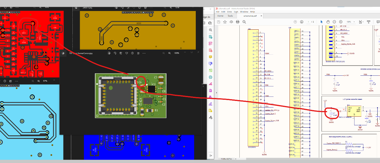
And, your resistors are also not in sync. R1 and R2 in the layout are for the Ic2 expander, but in the SCH, it is for your FLIR module and not R5/R6 as in the SCH:
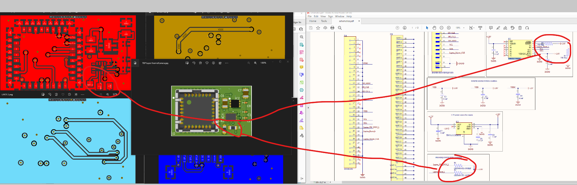
and there are a few other examples. So, I just think perhaps your layout reference designators are not synced to your design.J1 should be J2, and R3/R4 on the layout does not exist on the SCH.
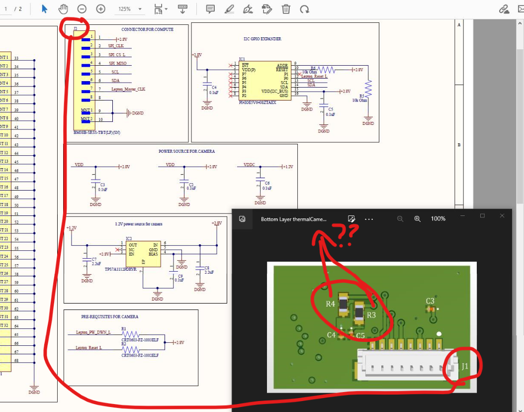
So, maybe this is where your issue is. I'd recheck the annotation between SCH and Layout, and be sure you are installing all the correct parts in the correct places.
Hope this helped!
Keep us posted.
Thanks! -
Hi @Jetson-Nano I have reviewed your schematic again and your layout files.
I cannot see any reason why your design will not work.
The only suggestion I have is to increase your capacitors here to 1uF:
But, otherwise, your layout is OK (some improvements can be made, but nothing is detrimental):
- Pin 1 correct on connector, socket, LDO, other ICs
- Vias are picking up planes correctly
- Voids where expected
- Generous copper trace thickness
The one issue I think I might have found is your reference designators do not match the schematic between the layout. So, I'm wondering if you are installing parts from the BOM in incorrect locations...
For example, the cap on the output of the LDO is "C6" in the layout, but "C7" in your schematic:
And, your resistors are also not in sync. R1 and R2 in the layout are for the Ic2 expander, but in the SCH, it is for your FLIR module and not R5/R6 as in the SCH:
and there are a few other examples. So, I just think perhaps your layout reference designators are not synced to your design.J1 should be J2, and R3/R4 on the layout does not exist on the SCH.
So, maybe this is where your issue is. I'd recheck the annotation between SCH and Layout, and be sure you are installing all the correct parts in the correct places.
Hope this helped!
Keep us posted.
Thanks!Hello @Vinny,
Hi Vinny,
Thank you again for your valuable feedback on the schematics and layout.
Apologies for not sending the updated files — the issues you pointed out were caused by that omission. I have now incorporated your suggestions and attached the updated schematics for your reference. I will also update the capacitor values to 1 µF as discussed.
Could you please review the attached schematics and let me know if any further changes are required?
Thanks very much for your continued support.
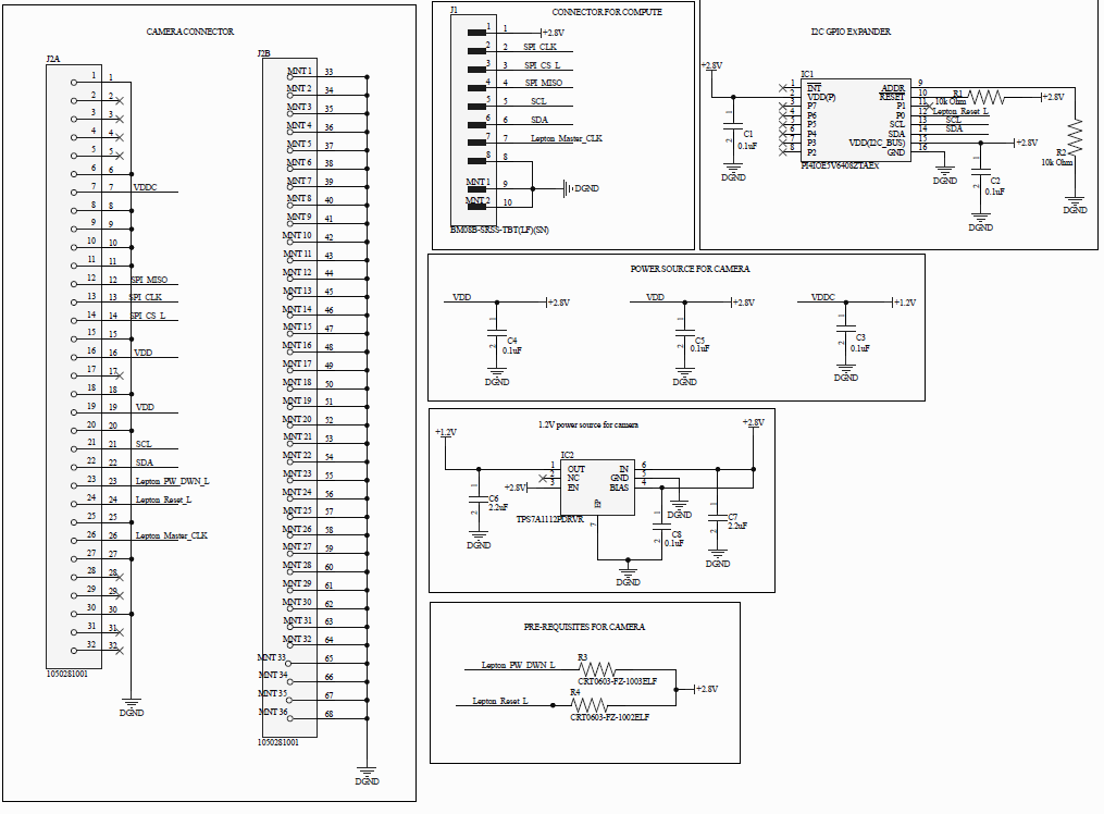
-
Hello @Vinny,
Hi Vinny,
Thank you again for your valuable feedback on the schematics and layout.
Apologies for not sending the updated files — the issues you pointed out were caused by that omission. I have now incorporated your suggestions and attached the updated schematics for your reference. I will also update the capacitor values to 1 µF as discussed.
Could you please review the attached schematics and let me know if any further changes are required?
Thanks very much for your continued support.
HI @Jetson-Nano
Your welcome. Apologies I cannot find anything blatantly wrong with your design at the document and layout level.
If your PCB still does not work after all these reviews and positive affirmations, then you may very well have a fabrication issue with your PCB.
The only way to verify that is to try your own net-by-net buzz-out using a DMM to ensure your netlist matches the expected schematic. If that all matches up, then you may be suffering from poor assembly/soldering. The socket for the lepton does require a reflow oven/line and cannot be hand soldered, unless you have an IR tray/heater and a way to deposit solder paste on the pads.Any further debugging I could offer would require physical samples of the hardware to validate everything.
Hope that info helps!
-
HI @Jetson-Nano
Your welcome. Apologies I cannot find anything blatantly wrong with your design at the document and layout level.
If your PCB still does not work after all these reviews and positive affirmations, then you may very well have a fabrication issue with your PCB.
The only way to verify that is to try your own net-by-net buzz-out using a DMM to ensure your netlist matches the expected schematic. If that all matches up, then you may be suffering from poor assembly/soldering. The socket for the lepton does require a reflow oven/line and cannot be hand soldered, unless you have an IR tray/heater and a way to deposit solder paste on the pads.Any further debugging I could offer would require physical samples of the hardware to validate everything.
Hope that info helps!
-
HI @Jetson-Nano
Your welcome. Apologies I cannot find anything blatantly wrong with your design at the document and layout level.
If your PCB still does not work after all these reviews and positive affirmations, then you may very well have a fabrication issue with your PCB.
The only way to verify that is to try your own net-by-net buzz-out using a DMM to ensure your netlist matches the expected schematic. If that all matches up, then you may be suffering from poor assembly/soldering. The socket for the lepton does require a reflow oven/line and cannot be hand soldered, unless you have an IR tray/heater and a way to deposit solder paste on the pads.Any further debugging I could offer would require physical samples of the hardware to validate everything.
Hope that info helps!
Hello @Vinny, @Alex-Kushleyev,
I am pleased to inform you that we have successfully manufactured the board and tested it today.
Everything worked as expected, and we were able to get the feed.
I sincerely thank you for your support and guidance throughout this process.
Thank you for your continued support.
-
Hello @Vinny, @Alex-Kushleyev,
I am pleased to inform you that we have successfully manufactured the board and tested it today.
Everything worked as expected, and we were able to get the feed.
I sincerely thank you for your support and guidance throughout this process.
Thank you for your continued support.
@Jetson-Nano
YES!!! So happy to hear that.


Reading along? Create a free ModalAI Forum account to join in.
With an account you can reply, ask your own question, get an email when a ModalAI engineer answers, and mark the reply that solved it. Your place in each thread is saved between visits.
Questions about VOXL, Flight Core, ESCs and ModalAI drones are answered here by the engineers who build them.
Register Login